- 您现在的位置:买卖IC网 > Sheet目录3870 > PIC16F1946-I/PT (Microchip Technology)IC MCU 8BIT FLASH 64TQFP
2010-2012 Microchip Technology Inc.
DS41414D-page 173
PIC16(L)F1946/47
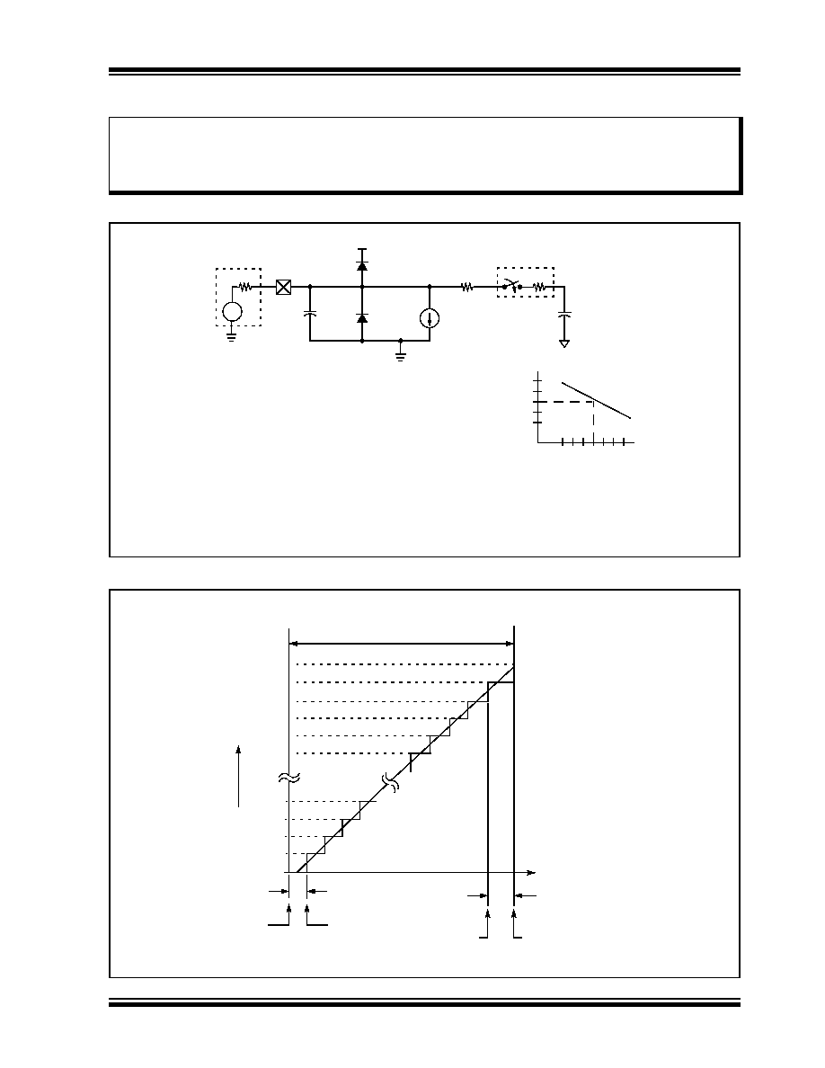
FIGURE 16-4:
ANALOG INPUT MODEL
FIGURE 16-5:
ADC TRANSFER FUNCTION
Note 1:
The reference voltage (VREF) has no effect on the equation, since it cancels itself out.
2:
The charge holding capacitor (CHOLD) is not discharged after each conversion.
3:
The maximum recommended impedance for analog sources is 10 k
. This is required to meet the pin
leakage specification.
CPIN
VA
Rs
Analog
5 pF
VDD
VT
0.6V
VT
0.6V
I LEAKAGE(1)
RIC
1k
Sampling
Switch
SS Rss
CHOLD = 10 pF
VSS/VREF-
6V
Sampling Switch
5V
4V
3V
2V
567 8 9 10 11
(k
)
VDD
Legend:
CPIN
VT
I LEAKAGE
RIC
SS
CHOLD
= Input Capacitance
= Threshold Voltage
= Leakage current at the pin due to
= Interconnect Resistance
= Sampling Switch
= Sample/Hold Capacitance
various junctions
RSS
Note 1: Refer to Section 30.0 “Electrical Specifications”
.
RSS
= Resistance of Sampling Switch
Input
pin
3FFh
3FEh
ADC
O
u
tput
Code
3FDh
3FCh
03h
02h
01h
00h
Full-Scale
3FBh
0.5 LSB
VREF-
Zero-Scale
Transition
VREF+
Transition
1.5 LSB
Full-Scale Range
Analog Input Voltage
发布紧急采购,3分钟左右您将得到回复。
相关PDF资料
PIC16LF1939-I/ML
IC MCU 8BIT FLASH 44QFN
PIC18LF6493-I/PT
IC PIC MCU FLASH 8KX16 64TQFP
DSPIC33FJ64GP310T-I/PT
IC DSPIC MCU/DSP 64K 100TQFP
DSPIC33FJ64GP310T-I/PF
IC DSPIC MCU/DSP 64K 100TQFP
PIC16C622A-20I/SO
IC MCU OTP 2KX14 COMP 18SOIC
PIC18LF14K50-I/SO
IC PIC MCU FLASH 16KB 20-SOIC
XF2M34151L
CONN FPC 34POS 0.5MM PITCH SMD
XF2M30151L
CONN FPC 30POS 0.5MM PITCH SMD
相关代理商/技术参数
PIC16F1946T-I/MR
功能描述:8位微控制器 -MCU 14KB 512B RAM 256B EEPROM RoHS:否 制造商:Silicon Labs 核心:8051 处理器系列:C8051F39x 数据总线宽度:8 bit 最大时钟频率:50 MHz 程序存储器大小:16 KB 数据 RAM 大小:1 KB 片上 ADC:Yes 工作电源电压:1.8 V to 3.6 V 工作温度范围:- 40 C to + 105 C 封装 / 箱体:QFN-20 安装风格:SMD/SMT
PIC16F1946T-I/PT
功能描述:8位微控制器 -MCU 14KB Flash, 512B RAM LCD, 1.8-5.5V RoHS:否 制造商:Silicon Labs 核心:8051 处理器系列:C8051F39x 数据总线宽度:8 bit 最大时钟频率:50 MHz 程序存储器大小:16 KB 数据 RAM 大小:1 KB 片上 ADC:Yes 工作电源电压:1.8 V to 3.6 V 工作温度范围:- 40 C to + 105 C 封装 / 箱体:QFN-20 安装风格:SMD/SMT
PIC16F1947-E/MR
功能描述:8位微控制器 -MCU 28KB1KB RAM 256B EEPROM RoHS:否 制造商:Silicon Labs 核心:8051 处理器系列:C8051F39x 数据总线宽度:8 bit 最大时钟频率:50 MHz 程序存储器大小:16 KB 数据 RAM 大小:1 KB 片上 ADC:Yes 工作电源电压:1.8 V to 3.6 V 工作温度范围:- 40 C to + 105 C 封装 / 箱体:QFN-20 安装风格:SMD/SMT
PIC16F1947-E/PT
功能描述:8位微控制器 -MCU 28KB Flash, 1KB RAM LCD, 1.8-5.5V RoHS:否 制造商:Silicon Labs 核心:8051 处理器系列:C8051F39x 数据总线宽度:8 bit 最大时钟频率:50 MHz 程序存储器大小:16 KB 数据 RAM 大小:1 KB 片上 ADC:Yes 工作电源电压:1.8 V to 3.6 V 工作温度范围:- 40 C to + 105 C 封装 / 箱体:QFN-20 安装风格:SMD/SMT
PIC16F1947-I/MR
功能描述:8位微控制器 -MCU 28KB1KB RAM 256B EEPROM RoHS:否 制造商:Silicon Labs 核心:8051 处理器系列:C8051F39x 数据总线宽度:8 bit 最大时钟频率:50 MHz 程序存储器大小:16 KB 数据 RAM 大小:1 KB 片上 ADC:Yes 工作电源电压:1.8 V to 3.6 V 工作温度范围:- 40 C to + 105 C 封装 / 箱体:QFN-20 安装风格:SMD/SMT
PIC16F1947-I/PT
功能描述:8位微控制器 -MCU 28KB Flash, 1KB RAM LCD, 1.8-5.5V RoHS:否 制造商:Silicon Labs 核心:8051 处理器系列:C8051F39x 数据总线宽度:8 bit 最大时钟频率:50 MHz 程序存储器大小:16 KB 数据 RAM 大小:1 KB 片上 ADC:Yes 工作电源电压:1.8 V to 3.6 V 工作温度范围:- 40 C to + 105 C 封装 / 箱体:QFN-20 安装风格:SMD/SMT
PIC16F1947T-I/MR
功能描述:8位微控制器 -MCU 28KB1KB RAM 256B EEPROM RoHS:否 制造商:Silicon Labs 核心:8051 处理器系列:C8051F39x 数据总线宽度:8 bit 最大时钟频率:50 MHz 程序存储器大小:16 KB 数据 RAM 大小:1 KB 片上 ADC:Yes 工作电源电压:1.8 V to 3.6 V 工作温度范围:- 40 C to + 105 C 封装 / 箱体:QFN-20 安装风格:SMD/SMT
PIC16F1947T-I/PT
功能描述:8位微控制器 -MCU 28KB Flash, 1KB RAM LCD, 1.8-5.5V RoHS:否 制造商:Silicon Labs 核心:8051 处理器系列:C8051F39x 数据总线宽度:8 bit 最大时钟频率:50 MHz 程序存储器大小:16 KB 数据 RAM 大小:1 KB 片上 ADC:Yes 工作电源电压:1.8 V to 3.6 V 工作温度范围:- 40 C to + 105 C 封装 / 箱体:QFN-20 安装风格:SMD/SMT